The Printed Circuit Board Assembly (PCBA) serves as the “central nervous system” for almost every modern piece of technology, from the smartphone in a pocket to satellites orbiting the planet.
While a bare board (PCB) provides the pathways for electricity, it is the assembly stage that transforms static components into an intelligent, functional system – the PCBA.
It’s worth mentioning that the term PCBA has two related meanings: it refers both to the process of mounting and soldering electronic components onto a bare PCB and to the finished, functional board that results from that process.
The scale of the market reflects how central PCBA has become to modern electronics. According to Meticulous Research, the global Printed Circuit Board Assembly market is projected to reach $147.5 billion by 2035, up from an estimated $90.91 billion in 2025.
But let’s first take a step back:
What Is A PCB?
A Printed Circuit Board (PCB) is the base where electronic components are mounted and interconnected to create the circuitry a device needs to function.
These multi-material boards form the stable foundation of a PCBA, directing current between active components, such as integrated circuits (ICs) like GPUs and memory chips, and passive components, such as resistors and capacitors, which help control or store electrical energy.
PCB Sizes
PCBs vary widely in size, from tiny boards used in wearables to larger boards manufactured on standard production panels. However, manufacturers often arrange boards on common production panels, such as 18 x 24 inches, to improve material use and scale production efficiently.
What Is A PCBA?
A PCBA (Printed Circuit Board Assembly) is a finished electronic assembly where all required components have been attached to a bare PCB. While the raw board provides the electrical pathways, the completed PCBA enables a device to process data, manage power, and perform its intended functions.
As a process, PCBA describes the mounting and soldering of electronic components onto a bare PCB. This transforms an inert board into a functioning electronic module by attaching active and passive components through precise soldering techniques.
PCBA is a core part of modern electronics, with the global Printed Circuit Board Assembly market projected to reach $147.5 billion by 2035.
What Is Soldering?
Soldering is the process of joining electronic components to a PCB using melted metal alloy called solder, often made from tin mixed with silver, copper, or other metals. When it cools, it forms a solid electrical and mechanical connection.
Printed Circuit Board Assembly: Past & Present
Through the years, there has been a significant shift in PCBA manufacturing.
In the past, complex electronic devices such as televisions and radios were meticulously wired by hand. These early devices used materials like Masonite before the arrival of modern phenolic boards in the 1950s.
Today, the process has moved from manual wiring to sophisticated, highly automated PCB assembly using materials such as FR-4 fiberglass-epoxy, PTFE-based laminates, and polyimide to meet the demands of miniaturization and precision.
Layer Architecture in Modern Electronic Board Assembly Design
A printed circuit board can consist of a single conductive layer or a complex stack of many layers, depending on the requirements of the final device.
Single-Sided Boards
These are the simplest form, featuring one layer of conducting material and a solder mask. Because they are easy to assemble and cost-effective, they are frequently used by hobbyists and for less complex electronic applications.
Double-Sided Boards
These boards have conductive layers on both the top and bottom, offering greater flexibility and a more compact size than single-layer versions. They are common in devices requiring more circuit complexity than a basic single-sided design can provide.
Single or double-layer boards are used for simple items like remote controls or basic LED bulbs.
Multi-Layer Boards
Multi-layer PCBs are the backbone of nearly all modern consumer electronics. They enable core features like high-speed processors, wireless connectivity, or a compact design.
Such boards typically range from 4 to 12 layers to balance performance with manufacturing costs. For example, mid-range smartphones use 8 to 10 layers to pack processors, RAM, and cameras into a slim frame.
Laptop motherboards often utilize 6 to 10 layers to manage complex signal routing between the CPU, GPU, and high-speed memory while maintaining stable power delivery.
PCB Assembly Methods: SMT (Surface-Mount Technology) and THT (Through-Hole Technology)
The printed circuit board assembly process generally utilizes two primary techniques, often coexisting on a single board.
Through-Hole Technology (THT)
THT involves component leads passing through plated through-holes (PTH) and being soldered on the opposite side to create a mechanical anchor.
It is often used for high-reliability products, especially in rugged environments:
- High-power and industrial electronics
- Outdoor signage
- Automotive electronics
- High-end, professional audio equipment
Indeed, PCBs with THT components can offer stronger vibration resistance, greater durability in harsh environments, better mechanical endurance, and improved thermal stability compared to surface-mount components.
Surface-Mount Technology (SMT)
SMT mounts components directly onto the surface of the board without the need for drilled holes. Components are secured on the PCB using a solder paste that is precisely applied to flat copper pads via a stencil.
Once the parts are placed, the entire board is passed through a reflow oven, which melts the paste to create permanent electrical and mechanical bonds.
The SMT method is the industry standard for high-volume manufacturing and devices that require extreme miniaturization, such as smartphones and IoT sensors.
By allowing components to be placed on both sides of the board, SMT supports higher component density while reducing the overall size and weight of sophisticated electronic devices.
It can also improve signal integrity by shortening connection paths and reducing the electrical noise, parasitic effects, and signal delays associated with longer through-hole leads.
The Printed Circuit Board (PCB) Assembly Process
The PCB assembly process can vary significantly depending on the production environment. In high-volume PCBA manufacturing, fully automated industrial lines help deliver professional-grade reliability, repeatability, and economies of scale.
Let’s take a look at how the basic electronic board assembly process typically unfolds on the shop floor.
Step 1: Design File and BOM Review
Before the first component is placed, teams need to confirm that the design, materials, boards, and components are ready for production, reducing the risk of scrap, rework, soldering defects, and reliability issues during the actual assembly process.
This typically involves:
- Reviewing Gerber files, which map out the copper layers and solder masks.
- Reviewing the Bill of Materials (BOM) that lists every necessary component.
- Perform Design for Manufacturability (DFM) that analyzes the raw board layout to identify copper slivers, narrow gaps, or spacing issues that could cause defects during fabrication.
- Perform Design for Assembly (DFA) in order to evaluate component placement and clearances, and ensure the board can be efficiently populated by automated machinery without errors.
Catching errors at this stage is essential for avoiding expensive board revisions later.
Step 2: Solder Paste Stenciling and Application
The first physical step in PCB assembly is applying solder paste to the board’s designated pads.
Assembly teams typically use a thin stainless-steel stencil as a mask, so the paste lands only where components will later sit. The paste is a greyish mixture of tiny solder particles, often made from tin, silver, and copper, combined with chemical flux.
Flux plays an important role because it helps clean oxidation from the metal surfaces and allows the solder to bond properly to the pads.
Precision is paramount here, as the volume and alignment of the paste determine the quality of the final electrical connection.
Step 3: Pick and Place
Once the solder paste is applied, the board moves to a pick-and-place machine, a high-speed robotic system that populates the board with Surface Mount Devices (SMDs). These machines use vacuum nozzles and other placement tools to pick tiny parts from reels or trays and position them onto the solder paste with extreme accuracy.
Advanced vision systems allow these robots to verify component alignment in real-time, making the mass production of densely packed circuit boards – like those in smartphones – possible.
Step 4: Reflow Soldering
After placement, the components need to be permanently attached to the circuit board.
Reflow soldering does this by heating the previously applied solder paste until it melts, or “reflows,” around the component leads and pads. As the board cools, the solder hardens and creates a permanent electrical and mechanical bond.
A standard reflow oven moves the board through four zones:
- Preheating activates the flux.
- Thermal soak stabilizes component temperatures.
- Reflow raises the heat enough to melt the solder.
- Cooling solidifies the solder joints.
For high-reliability or highly miniaturized boards, assembly teams may use a nitrogen atmosphere to reduce oxidation during soldering.
They also tailor the oven’s thermal profile to the board size and component sensitivity, helping prevent heat damage while ensuring the solder melts properly.
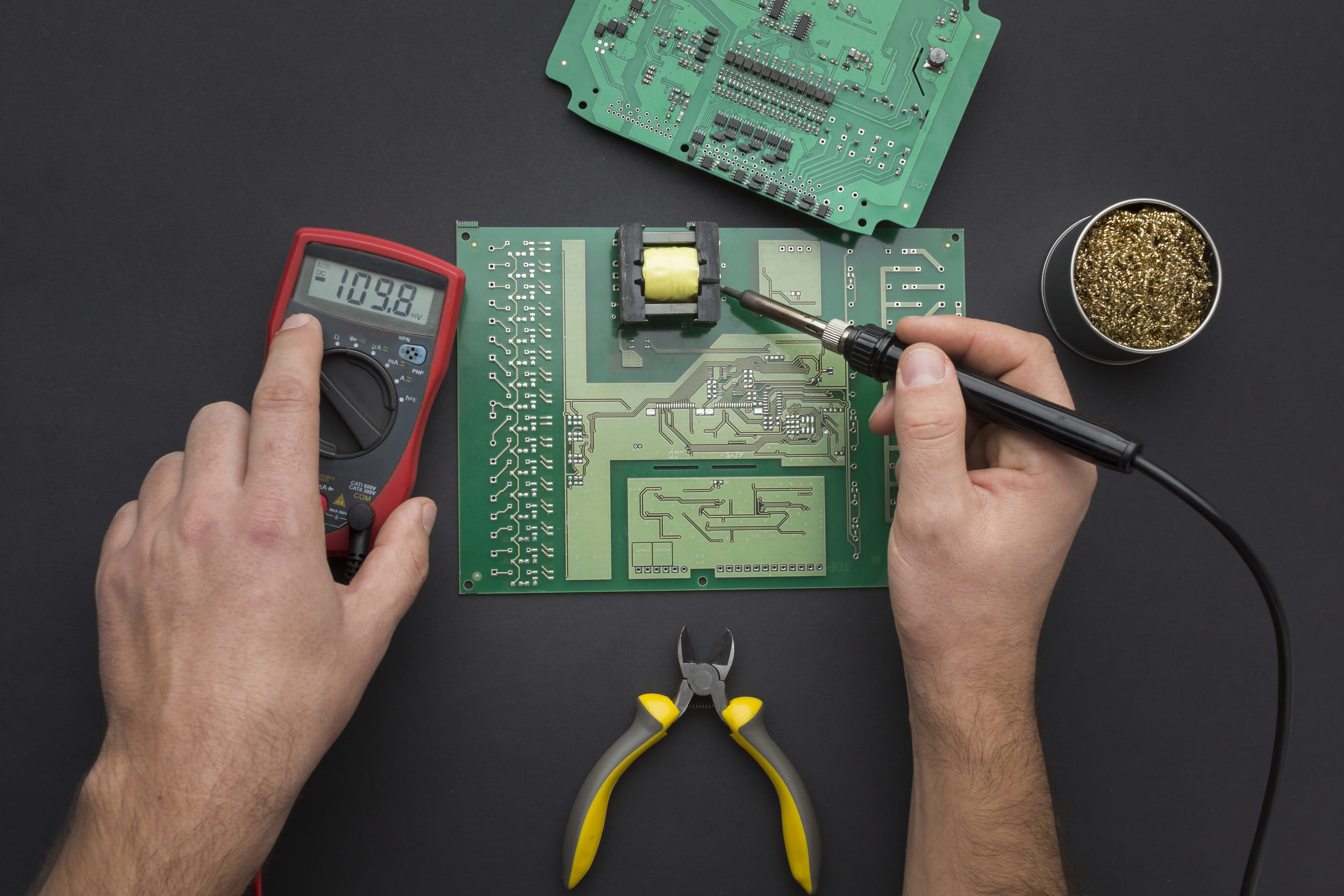
Step 5: Inspection and Quality Control
The electronic board assembly must go through rigorous inspection to confirm that components are correctly placed, solder joints are reliable, and the board meets its required quality standards.
Several inspection steps take place throughout the line.
For example, Solder Paste Inspection (SPI) checks paste volume and alignment after stenciling, while visual or automated checks may happen before the board enters the reflow oven. After reflow, Automated Optical Inspection (AOI) uses high-resolution cameras to scan for missing parts, misaligned components, incorrect polarity, tombstoning, and solder bridges.
Finally, In-Circuit Testing (ICT) or Functional Testing runs power and signals through the board to verify that every component is electrically sound and performs as intended. This layered quality-control process ensures that any defects are caught and rectified before the PCBA reaches final product integration.
Step 6: Cleaning, Packaging, and Shipping
The final steps in the PCBA process focus on cleaning, protecting, and preparing the finished assembly for safe storage, handling, and delivery.
Boards are often cleaned with deionized water or specialized cleaning solutions to remove flux residue, oils, and other contaminants that could cause corrosion, performance issues, or cosmetic defects.
After drying, the boards may be coated with a thin protective layer that helps shield the PCBA from moisture, dust, vibration, and harsh operating conditions.
Proper packaging is the final line of defense. Ready-to-ship PCBAs are placed in anti-static bags, trays, foam inserts, or specialized ESD-safe containers to reduce the risk of static discharge, physical shock, contamination, or handling damage during storage and transit.
Recent industry data also points to resilient demand. North American PCB shipments rose 21.4% year over year last May, while the book-to-bill ratio stood at 1.03 – meaning orders remained slightly ahead of shipments.
As volumes rise, consumer electronics brands need tighter control over storage, packaging, and shipment planning.
This is where an experienced electronics logistics provider becomes especially valuable.
Where Electronics Logistics Takes Over
PCBA and finished-device shipments often need more than standard pick, pack, and ship workflows. They may require ESD-safe handling, controlled storage, protective packaging, inventory visibility, kitting, accessory matching, returns management, and testing support before reaching customers or retail channels.
Green Wave Electronics is built around these post-assembly requirements.
With electronics-focused repackaging services, ESD-safe handling, controlled storage, and expert fulfillment support, Green Wave Electronics helps consumer electronics brands protect product integrity after assembly and keep inventory moving safely, efficiently, and cost-effectively.
When the board is finished, the product journey is just getting started. Talk to our team.